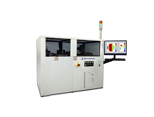

UltraMap UMA-C200 System with full automation including robotic loading and 6 cassettes for binning.A convenient benchtop version, the UltraMap UMB-C200, is also available.Designed specifically for high throughput dimensional measurement of sapphire wafers for HB-LED manufacturing, the UltraMap C200 provides throughput of ninety 6” diameter sapphire wafers per hour with lowest cost of ownership (CoO). The UltraMap C200 utilizes MicroSense’s novel two sided capacitive sensing technology to measure sapphire wafer thickness, TTV (total thickness variation), bow, warp, and LTV (local thickness variation).
More than 100,000 measured points per 6" wafer, with no sacrifice in throughput
Thickness and Global Flatness Measurements - TTV, TIR, FPD
Local Flatness: Local Thickness Variation (LTV), LTIR, LFPD
Bow, Warp and SORI
Throughput - up to 90 6" wafers per hour
0.05 micron thickness repeatability
2D and 3D mapping