


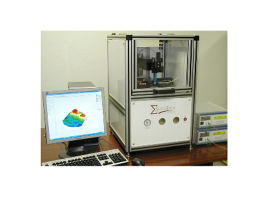
The UltraMap-100 system make automatic, non-contact measurement of thickness, flatness and shape of wafers up to 4" diameter with this compact system.The system very repeatably measures wafer thickness, TTV, and shape in compliance with SEMI standards.Measure with sub-micron resolution and repeatability.
Exclusive non-contact sensing technology with dual White light chromatic coding probes (10nm resolution)
System accepts wafer sizes from 1” to 4” diameter (25 to 100mm). Thickness range - 50um to 3mm
User selectable number of measurement points
UltraMap measurement software features 2D & 3D mapping along with data export
Wafer positioning and wafer measurement are fully automatic. Wafers are manually loaded into the wafer holder.
The system features in machine automated calibration.
Economical yet full featured system for measuring smaller substrates


