


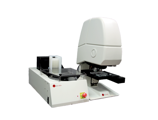
A fully automated, optical inspection system for analyzing opaque, transparent, and semi-transparent wafers for defects.
nSPEC® offers fast quantification and qualification of defects with detailed reporting and mapping.
nSPEC® can image and analyze substrate and epi wafers as well as patterned and diced wafers as well as individual devices.
The system has multiple magnifications to fully characterize defect frequency and type.
nSPEC® also offers complete rapid scanning and mosaicing of wafers. Users can easily define reports and statistical functions.
Optics
White light illumination LED
Bright field/dark field objectives 5x and 10x, other magnifications optional
Differential interference contrast Nomarski
Polarization and analyzer Included
Stage
Travel, typical 200mm X and Y direction
Centered load capability 5 lb.
Repeatability +/- 2μm
Construction a) Precision ground alum plates.
b) Stainless steel raceways with cross roller bearings
Resolution +/- 2μm
Travel flatness Better than 30μm
Weight 12 lb.
Limit switches Mechanical, non-adjustable
Wafer chucks 100 and 150mm, other sizes optional
Warranty 1 year
Standard Camera
Pixel size,typical 4.54μm
Image size 2752x 2000 pixels minimum
Maximum frame rate 8fps
Control (computer included with purchase of nSPEC®)
Stage Computer and joystick controlled
Focus Automated and manual
Nosepiece Computer controlled
Illumination Computer controlled
Camera Automated and manual


