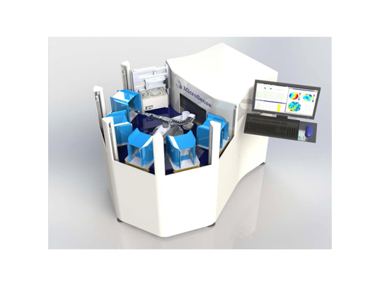

Precise Automated Measurement for High Volume Silicon Wafer Manufacturing
High Repeatablity, Industry Standard Measurement of:
Wafer Global Flatness and Site Flatness
Wafer Thickness
Wafer Shape – Bow, Warp, SORI
Wafer Resistivity and Wafer P/N Type
High Throughput System
Measure 32% more wafers per shift compared to ADE 9600
• Reduce 200mm wafer measurement time – industry leading 1.25x higher throughput – 56 wafers per hour, with full wafer mapping and 2mm edge exclusion
• Nanometer resolution, dual probe MicroSense capacitive measurement system for high sensitivity and high repeatability measurements in compliance with SEMI standards
• Measures over 200,000 data points per 200mm wafer
• Fully automated in machine Auto-Calibration – more wafers measured each shift
• Designed for reliability and long term support - UltraMap has a modern, high reliability system design with direct drive precision air bearing r-theta wafer stage and software running on Windows computer.
• Ease of Integration - UltraMap wafer data is output in a variety of industry standard formats and is compatible with existing data management in your factory